Trade Lam Research Corporation - LRCX
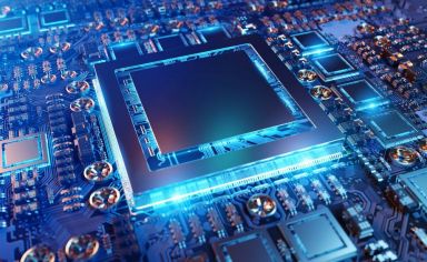
Lam Research Corporation designs, manufactures, markets, refurbishes, and services semiconductor processing equipment used in the fabrication of integrated circuits worldwide. The company offers thin film deposition products, including SABRE electrochemical deposition products for copper damascene manufacturing; ALTUS systems to deposit conformal atomic layer films for tungsten metallization applications; VECTOR plasma-enhanced chemical vapor deposition (CVD) and atomic layer deposition systems to deposit oxides, nitrides, and carbides for hardmasks, multiple patterning films, anti-reflective layers, multi-layer stack films, and diffusion barriers; and Striker atomic layer deposition systems that deliver conformal dielectric films for spacer-based patterning and liner applications in various advanced memory and logic structures. Its thin film deposition products also comprise SPEED high-density plasma CVD products for applications in shallow trench isolation, pre-metal dielectrics, inter-layer dielectrics, inter-metal dielectrics, and passivation layers; and SOLA ultraviolet thermal processing products for treatment of back-end-of-line (BEOL) low-k dielectric films and front-end-of-line silicon nitride strained films. In addition, the company offers plasma etch products, such as Kiyo that provide solutions for conductor etch applications; Versys metal products, which offer a platform for BEOL metal etch processes; Flex for dielectric etch applications; and Syndion to address various through-silicon via etch and complementary image sensor etch applications. Further, it provides single-wafer clean products comprising EOS, Da Vinci, DV-Prime, and SP series products for wet etch and clean applications in wafer-level packaging; and Coronus plasma-based bevel clean products to enhance die yield by removing particles, residues, and unwanted films from the wafer's edge, as well as legacy products. The company was founded in 1980 and is headquartered in Fremont, California.Latest shares articles
Lam Research stock split: what it means for traders
Lam Research’s 2024 stock split followed earlier adjustments to its share structure and reflects a long-standing approach to managing how its equity is issued and traded.
14:59, 16 December 2025

Michael Kramer: Why Do Revisions Matter So Much in the Payroll Report?
The most important number in the monthly US non-farm payroll report may not be the headline payroll figure, but the revisions that follow months later.
13 hours ago

Michael Kramer: Why Is Trimmed Mean PCE Kevin Warsh's Preferred Inflation Gauge?
What gets called 'inflation' in the headlines is really the change in a price index — and how that index is built shapes the number.
13 hours ago

Michael Kramer: What Can Options Positioning Tell Us About Post-Earnings Moves? Nvidia as an Example
Options positioning and implied volatility are data points that analysts observe ahead of earnings events.
15 hours ago
Related News
Public Technologies•Europe
16:56 (UTC), 14 July 2026Public Technologies•Europe
20:06 (UTC), 8 July 2026Public Technologies•Europe
16:34 (UTC), 6 July 2026